Introduction
Yesterday TSMC unveiled its newest semiconductor process, advanced packaging, and 3D IC technologies for powering the next generation of AI innovations with silicon leadership at the Company’s 2024 North America Technology Symposium.
TSMC debuted the TSMC A16™ technology, featuring leading nanosheet transistors with innovative backside power rail solution for production in 2026, bringing greatly improved logic density and performance. TSMC also introduced its System-on-Wafer (TSMC-SoW™) technology, an innovative solution to bring revolutionary performance to the wafer level in addressing the future AI requirements for hyperscaler datacenters.
Read more 5 Major Takeaways from TSMC Impressive Q1 FY24 Results – techovedas
TSMC Symposium Highlights
This year marks the 30th anniversary of TSMC’s North America Technology Symposium, and more than 2,000 attended the event, growing from less than 100 attendees 30 years ago. The North America Technology Symposium in Santa Clara, California kicks off TSMC Technology Symposiums around the world in the coming months. The symposium also featured an “Innovation Zone,” designed to highlight the technology achievements of our emerging start-up customers.
We are entering an AI-empowered world, where artificial intelligence not only runs in data centers, but PCs, mobile devices, automobiles, and even the Internet of Things,”
Dr. C.C. Wei, TMSC CEO
New Technologies introduced in the TSMC Symposium
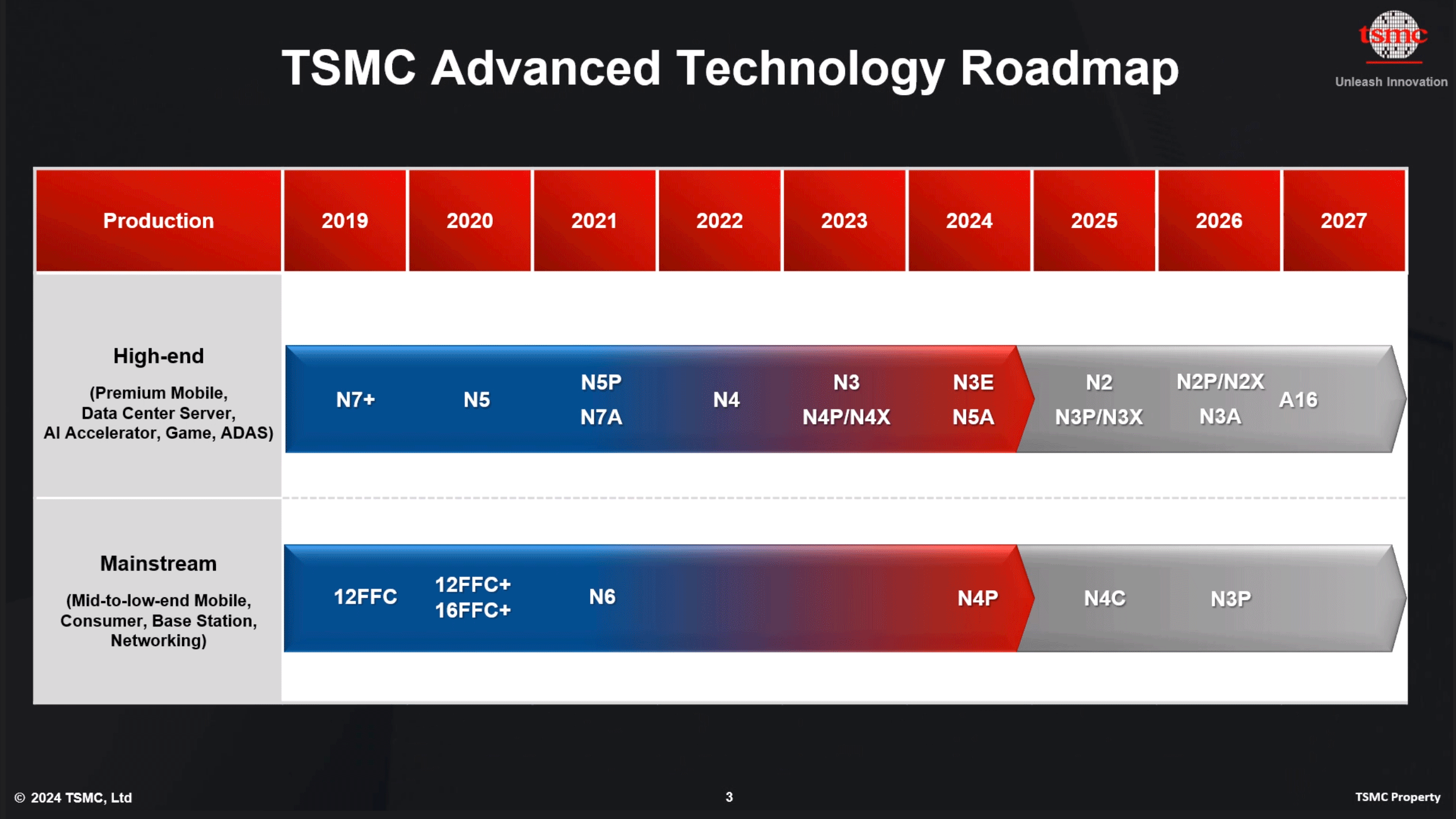
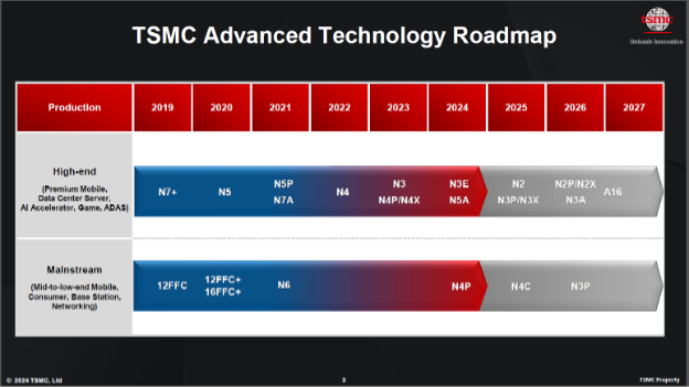
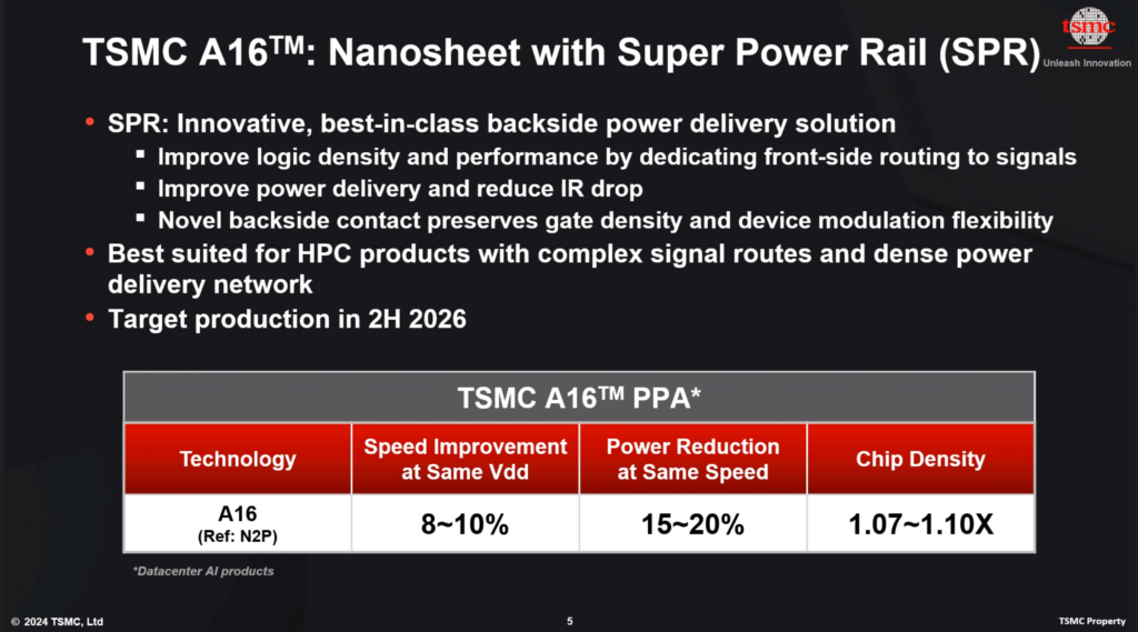
1. TSMC introduced its A16™ Technology in Symposium
The next milestone in its semiconductor roadmap, the A16 (1.6nm) builds on the success of N3E technology currently in production and with N2 (2nm) slated for release in late 2025, A16 combines TSMC’s innovative Super Power Rail architecture with nanosheet transistors. This combination is set to enhance logic density and performance by allocating front-side routing resources specifically to signals.
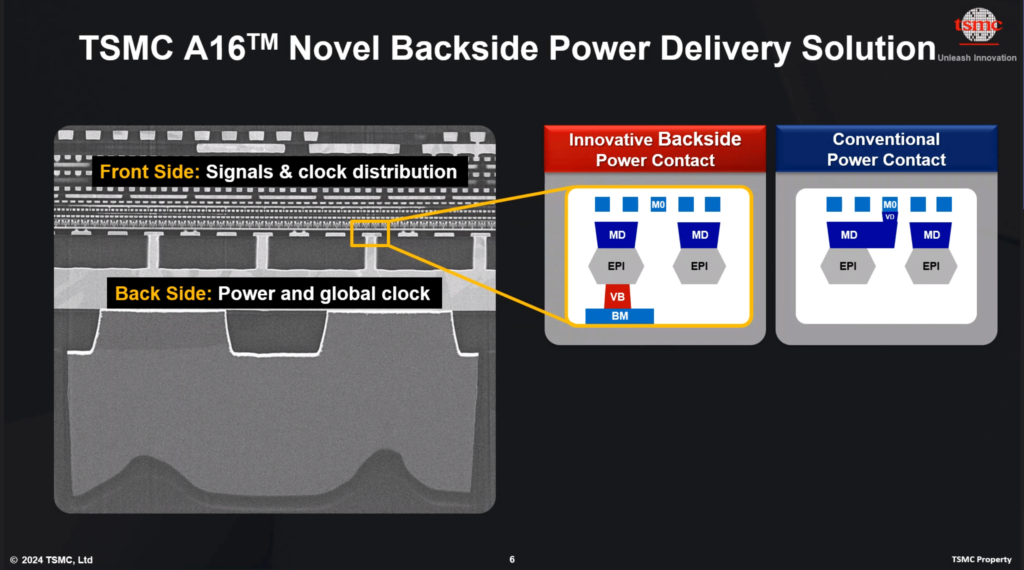
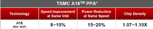
A16 is particularly suited for High Performance Computing (HPC) products, boasting intricate signal routes and dense power delivery networks. Compared to TSMC’s N2P process, A16 promises significant improvements: an 8-10% speed enhancement at the same positive power supply voltage (Vdd), a 15-20% reduction in power consumption at the same speed, and up to a 1.10X increase in chip density, tailored especially for data center products.
Read more TSMC 2nm Trial Production To Begin in 2024; HVM by 2025 – techovedas
2. TSMC Nanoflex for Nanosheet transistors
TSMC also unveiled its NanoFlex™ Innovation for Nanosheet Transistors, accompanying the upcoming N2 technology. This new N2 process is scheduled for 2025 and will have a capability like N3’s FinFlex technology, called NanoFlex. This will allow the mixing of short cells and tall cells in the same block to get better PPA by mixing in the best ratio of cells for any given design. Figure below shows the advantages of a mixed height design over a short cell only implementation.
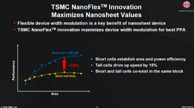
This flexibility allows customers to fine-tune their designs, achieving optimal power, performance, and area tradeoffs for their specific applications.
3. N4C technology at TSMC Symposium
Furthermore, TSMC introduced N4C Technology, an extension of its N4P technology aimed at a broader range of applications.
N4C promises up to an 8.5% reduction in die cost with minimal adoption effort, scheduled for volume production in 2025. It offers area-efficient foundation IP and design rules fully compatible with N4P, delivering better yield through die size reduction. This provides a cost-effective option for migrating value-tier products to TSMC’s next advanced technology node.
N4 is tsmc’s 4nm technology. After N4, TSMC released N4P technology which improved N4’s performance by 6%. And now we have N4C.
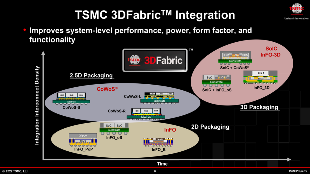
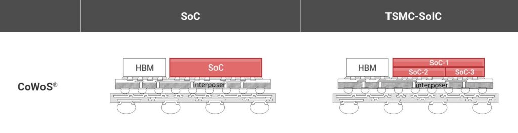
4. CoWoS, SoIC and System on Wafer (TSMC-SoW) in TSMC Symposium
In addition to these advancements, TSMC showcased its commitment to innovation in advanced packaging technologies such as CoWoS®, SoIC, and System-on-Wafer (TSMC-SoW™). CoWoS has played a pivotal role in the AI revolution by enabling customers to densely pack processor cores and high-bandwidth memory (HBM) stacks on a single interposer.
TSMC-SoW introduces a novel approach, enabling a large array of dies on a 300mm wafer, offering increased compute power while occupying significantly less data center space and enhancing performance per watt by several orders of magnitude.
5. Silicon Photonics integration at TSMC Symposium
TSMC also highlighted its efforts in Silicon Photonics Integration, introducing COUPE™ technology to support the surging demand for data transmission in the AI era. COUPE utilizes SoIC-X chip stacking technology to stack electrical and photonic dies, offering superior energy efficiency and reduced impedance at the die-to-die interface. TSMC plans to qualify COUPE for small form factor pluggables in 2025, followed by integration into CoWoS packaging as co-packaged optics (CPO) in 2026.
6. Automotive Advanced Packaging
Lastly, TSMC addressed Automotive Advanced Packaging, catering to the increasing computing power demands of automotive applications while meeting stringent safety and quality standards.
Developments such as InFO-oS and CoWoS-R solutions target applications like advanced driver assistance systems (ADAS), vehicle control, and vehicle central computers, aiming for AEC-Q100 Grade 2 qualification by the fourth quarter of 2025.
Read more 6 Leading Companies in Advanced Packaging of Integrated Circuits – techovedas
Summary
TSMC unveiled groundbreaking semiconductor advancements at its 2024 North America Technology Symposium, showcasing the A16™ Technology set for production in 2026, promising enhanced logic density and performance.
Additionally, TSMC introduced NanoFlex™ for Nanosheet Transistors and N4C Technology, aiming to optimize power, performance, and area tradeoffs. The symposium also highlighted innovative packaging technologies like CoWoS®, SoIC, and TSMC-SoW™, along with Silicon Photonics Integration and Automotive Advanced Packaging solutions. With a focus on powering the next generation of AI innovations, TSMC continues to lead in silicon technology through its innovative packaging offerings.