Introduction
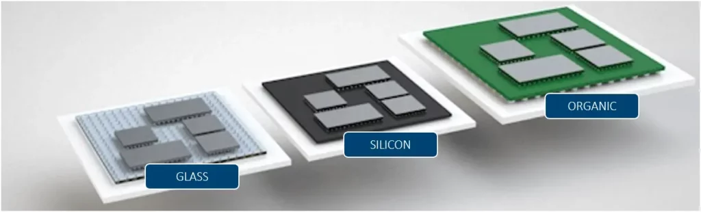
In the relentless pursuit of innovation, the semiconductor industry moving towards new substrate materials. Compared to today’s organic substrates, glass offers distinctive properties such as ultra-low flatness and better thermal and mechanical stability, resulting in much higher interconnect density in a substrate. These benefits will allow chip architects to create high-density, high-performance chip packages for data-intensive workloads such as artificial intelligence (AI).
Follow us on Linkedin for everything around Semiconductors & AI
Understanding Glass Vs Silicon Substrate
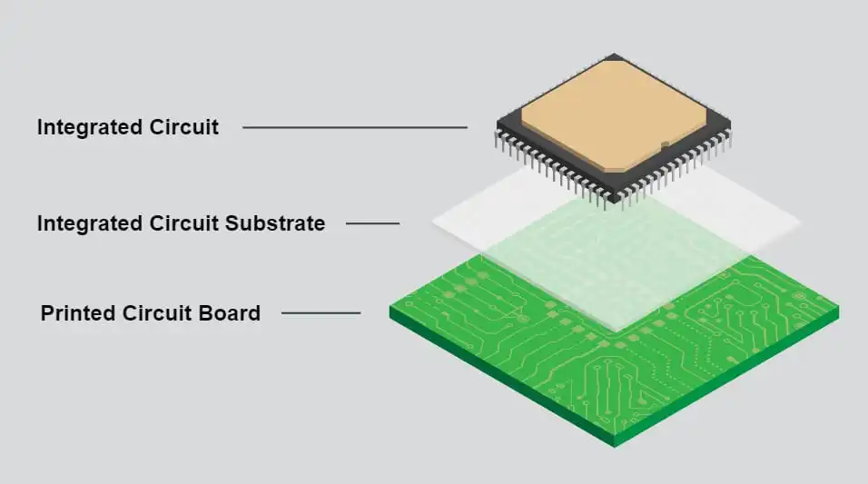
In semiconductor manufacturing, a substrate serves as the foundation upon which electronic components are fabricated. It provides structural support and electrical insulation while facilitating the deposition of thin-film materials necessary for semiconductor device fabrication. Historically, silicon has been the substrate material of choice due to its abundance, compatibility with semiconductor processing techniques, and desirable electrical properties.
Read More: Intel Promises 1 Trillion Transistors on a Chip by 2030 Using Glass Substrates
Difference between Substrate and PCBs
- Substrate: This is a part of the PCB. It’s like the foundation of a house. It provides a base for mounting electronic components and it also provides electrical insulation between the components.
- PCB: This is like the entire house. It includes the substrate (foundation), but also has other parts. These include the electronic components include capacitors, heat sinks and the copper traces that connect these components
Read more Career in PCB Design – techovedas
Transition from Conventional Substrates
While silicon has been instrumental in driving the semiconductor industry forward, the pursuit of further advancements has led to the exploration of alternative substrate materials. Glass has emerged as a compelling candidate owing to its unique properties, including excellent thermal stability, optical transparency, and scalability.
Traditional substrates like silicon faced limitations in handling complex interconnect layouts and heat dissipation. They risked distortion under high temperatures, compromising device integrity. Moreover, their surface irregularities hindered precise patterning, constraining interconnect density. These shortcomings necessitated the shift towards more robust alternatives like glass substrates.
Read more 5 Ways Chip Packaging Will Define Next Generation of Chips – techovedas
Benefits of Glass Substrate
Glass substrates present a significant advantage when it comes to thermal management in electronic devices. Unlike organic substrates that can unpredictably stretch and relax under temperature variations, glass substrates offer a higher level of stiffness and resistance to thermal warping. This added stability allows for the incorporation of more routing holes in the substrate, enabling increased power and data connections, as well as improved signal integrity.
1. Thermal Stability
The ability to tolerate higher temperatures is a notable characteristic that has impressed companies. Higher thermal stability allows them to use glass substrate in Data centres chips and AI workloads where computation tasks are demanding.
2. Higher interconnect density
Glass substrates are planar i.e. they have uniform thickness. A uniformly planar substrate allows precise patterning of interconnect layers, facilitating tight packing of interconnects. Thermal stability prevents warping or distortion during processing, enabling multiple layers of interconnects without compromising their integrity. Together, they allow for densely packed interconnect structures, achieving higher interconnect density on glass substrates.
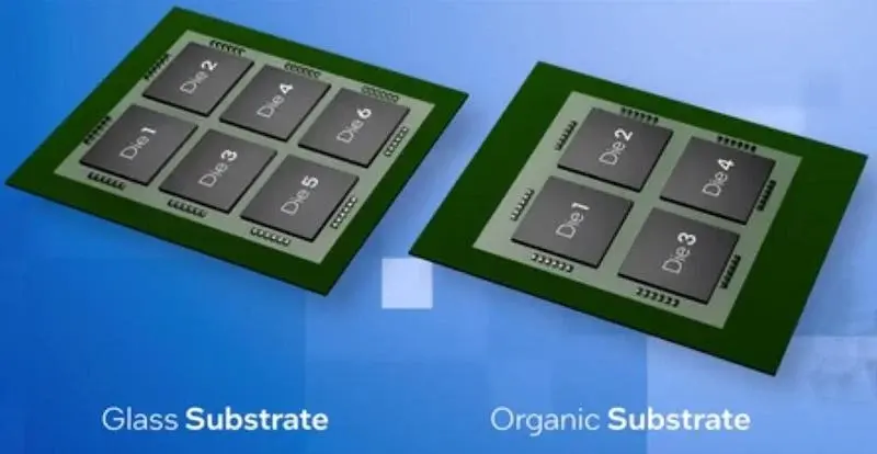
3. 50 % more die content
Glass substrate enables 50% more die content on the same package size than organic substrates. This is because their flat surface ensures chips fit snugly, reducing wasted space. Additionally they handle heat well, preventing warping and safeguarding delicate components. This stability, combined with precise manufacturing, promises streamlined, efficiently packed chiplets.
4. Chemical Inertness
Glass substrates are chemically inert, rendering them resistant to corrosion and degradation when exposed to harsh environmental conditions or chemical processes. This durability enhances the longevity and reliability of semiconductor devices, particularly in applications where exposure to corrosive agents is prevalent.
Read more AMD vs Intel: Which CPU Reigns Supreme in 2024? – techovedas
5. Flatness and Warp Management:
Glass is naturally flatter and stiffer than silicon. This makes it ideal as a carrier for thin silicon wafers during processing. The flatter surface helps prevent warping which can be a big issue with ultra-thin silicon wafers.
6. Cost-Effectiveness:
Glass substrates can be significantly cheaper than silicon wafers, especially for larger or thinner wafers. This can be a major advantage for non-critical processes or temporary support during manufacturing.
7. Transparency:
Because glass is transparent, it allows for easier inspection of the underlying silicon wafer. This is useful for monitoring processes like bonding or debonding during development.
Here’s a quick comparison:
| Feature | Glass Substrate | Silicon |
|---|---|---|
| Electrical Conductivity | Insulator | Semiconductor |
| Flatness | Superior | Good |
| Thermal Expansion | Tailorable | Fixed |
| Cost | Lower | Higher |
| Transparency | Transparent | Opaque |
Overall, glass substrates aren’t replacing silicon chips, but they serve a valuable purpose as a supportive platform during specific stages of semiconductor manufacturing, especially for thin and advanced devices.
Incorporation of Glass Substrate
Intel has been working on glass substrates for almost a decade. It has announced plans to adopt glass substrates for commercial products by 2030.
Integration of glass substrates into semiconductor manufacturing involves adapting existing fabrication processes to accommodate the unique properties of glass. Techniques such as sputtering, chemical vapor deposition (CVD), and physical vapor deposition (PVD) are employed to deposit thin-film materials onto glass substrates, enabling the realization of diverse semiconductor devices ranging from microelectronics to advanced photonic components.
Read more Samsung Plans to Commercialize Glass Substrate by 2026 – techovedas
Conclusion
In wrapping up, it’s evident that the semiconductor field is on the brink of a significant shift toward glass substrates. With their unparalleled thermal stability, increased interconnect density, and resistance to chemical degradation, glass substrates are poised to redefine the way electronic devices are made. The involvement of industry giants like Intel in spearheading this transition signals the dawn of a new era in semiconductor innovation. These advancements promise to unlock new levels of performance in chips tailored for the demanding landscapes of AI and data-centric applications.